STO on Silicon

Epitaxially grown strontium titanate on silicon substrates
STO (SrTiO3) on Si substrates

What we can offer you

  • 4nm crystalline oxide epitaxial layer deposited on Si substrate
  • Best-in-class quality and stability
  • Direct integration on silicon enbles scaling of your research/technology
  • Doped Si backside layer instead of Nb doping

... enabling your ...

  • project on oxide epitaxy with perovskites (e.g., ferroelectrics, multiferroics, colossal magnetoresistance, high-Tc superconductivity, ...)
  • research requiring layer transfer of STO
  • need for larger surfaces than what is possible with STO single crystals
  • MEMS processes fabricating membranes by underetching the Si substrate
  • Other applications: RF, sensing, spintronics, material science, ...
STO on Si
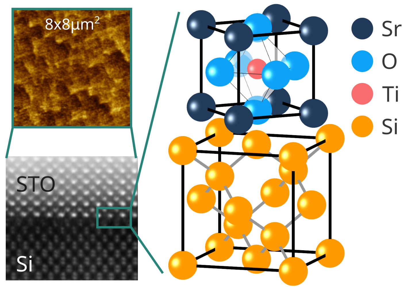
Bottom left: TEM image of the interface between Si substrate and STO apitaxial layer. Top left: 8x8 μm2 AFM image. The terraces have a height of ~2 Å. Right: Schematic of the crystal lattices with color coded atoms.

Specifications

Size
5x5, 10x10, 15x15 mm2 (other dimensions on request)
Thickness
725 ± 25 μm
Orientation
(001) ± 0.5°
Doping
p-type
Resistivity
1-30 Ωcm
SrTiO3 layer
4.0 ± 0.2 nm
Roughness
3 ± 2 Å
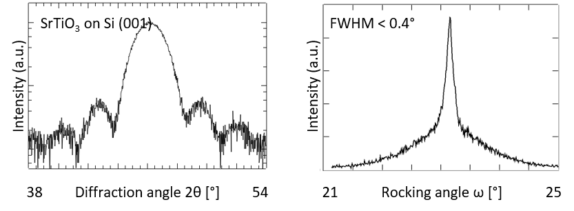
Mosaicity
0.4°
Max temp.
800°C
STO on Si specifications
Left: XRD analysis of STO epitaxial layer on Si. Right: rocking curve demonstrating a mosacitiy < 0.4°

References

Strain-Engineered Metal-to-Insulator Transition and Orbital in Nickelate Superlattices Integrated on Silicon, B. Chen et al., Adv. Mater., 2004995 (2020)

Integration of Single Oriented Oxide Superlattices on Silicon Using Various Template Techniques, B. Chen et al., ACS Appl. Mater. Interfaces, 12(38) 42925 (2020)

Thermal-strain-engineered ferromagnetism of LaMnO3/SrTiO3 heterostructures grown on silicon, B. Chen et al., Physical Review Materials 4, 024406 (2020)

Microstructure analysis of epitaxial BaTiO3 thin films on SrTiO3-buffered Si: Strain and dislocation density quantification using HRXRD methods, A.Borzì et al., Materialia, 14, 100953 (2020)

Monolithically Integrated Microelectromechanical Systems for On-Chip Strain Engineering of Quantum Dots, Y. Zhang et al., Nano Lett., 16(9), 5785 (2016)

Wafer level integration of epitaxial piezoelectric thin films for novel NEMS, MEMS and MOEMS applications, M. Dekkers et al., Informatics, Electronics and Microsystems: TechConnect Briefs (2017)


Overview of elements with access to our shop

1 18
H
2 13 14 15 16 17
He
Li Be B C
N
O
F
Ne
Na Mg 3 4 5 6 7 8 9 10 11 12 Al Si P S
Cl
Ar
K Ca Sc Ti V Cr Mn Fe Co Ni Cu Zn Ga Ge As Se
Br
Kr
Rb Sr Y Zr Nb Mo
Tc
Ru Rh Pd Ag Cd In Sn Sb Te I
Xe
Cs Ba La Hf Ta W Re Os Ir Pt Au Hg Tl Pb Bi
Po
At
Ra
Fr
Ra
Ac
Ce Pr Nd
Pm
Sm Eu Gd Tb Dy Ho Er Tm Yb Lu


Get our latest news and special sales
You may unsubscribe at any moment. For that purpose, please find our contact info in the legal notice.
Tel.: +49 (0) 2461 - 9352 - 0
Fax: +49 (0) 2461 - 9352 - 11