& Kristalle GmbH

-
 English
-
Deutsch
Keine Artikel
Gesamt zzgl. MwSt.
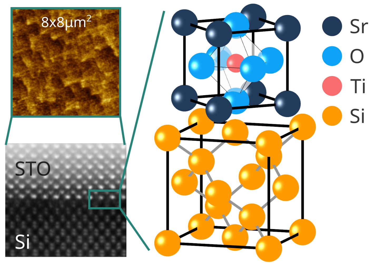
STO on Silicon
Epitaktisch gewachsenes Strontiumtitanat auf Silizium-Substraten
STO (SrTiO3) on Si substrates
What we can offer you
- 4nm crystalline oxide epitaxial layer deposited on Si substrate
- Best-in-class quality and stability
- Direct integration on silicon enbles scaling of your research/technology
- Doped Si backside layer instead of Nb doping
... enabling your ...
- project on oxide epitaxy with perovskites (e.g., ferroelectrics, multiferroics, colossal magnetoresistance, high-Tc superconductivity, ...)
- research requiring layer transfer of STO
- need for larger surfaces than what is possible with STO single crystals
- MEMS processes fabricating membranes by underetching the Si substrate
- Other applications: RF, sensing, spintronics, material science, ...
Specifications
- Size
- 5x5, 10x10, 15x15 mm2 (other dimensions on request)
- Thickness
- 725 ± 25 μm
- Orientation
- (001) ± 0.5°
- Doping
- p-type
- Resistivity
- 1-30 Ωcm
- SrTiO3 layer
- 4.0 ± 0.2 nm
- Roughness
- 3 ± 2 Å
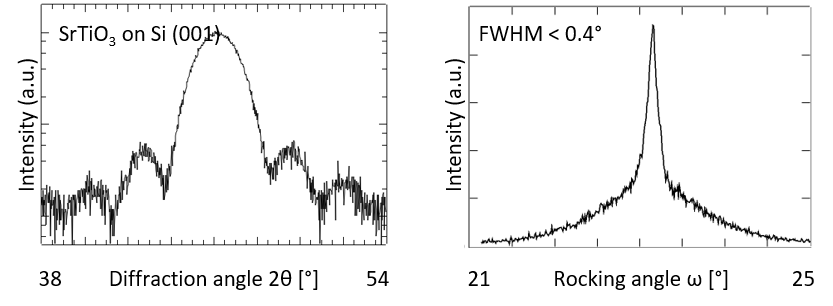
- Mosaicity
- 0.4°
- Max temp.
- 800°C
References
Strain-Engineered Metal-to-Insulator Transition and Orbital in Nickelate Superlattices Integrated on Silicon, B. Chen et al., Adv. Mater., 2004995 (2020)
Integration of Single Oriented Oxide Superlattices on Silicon Using Various Template Techniques, B. Chen et al., ACS Appl. Mater. Interfaces, 12(38) 42925 (2020)
Thermal-strain-engineered ferromagnetism of LaMnO3/SrTiO3 heterostructures grown on silicon, B. Chen et al., Physical Review Materials 4, 024406 (2020)
Microstructure analysis of epitaxial BaTiO3 thin films on SrTiO3-buffered Si: Strain and dislocation density quantification using HRXRD methods, A.Borzì et al., Materialia, 14, 100953 (2020)
Monolithically Integrated Microelectromechanical Systems for On-Chip Strain Engineering of Quantum Dots, Y. Zhang et al., Nano Lett., 16(9), 5785 (2016)
Wafer level integration of epitaxial piezoelectric thin films for novel NEMS, MEMS and MOEMS applications, M. Dekkers et al., Informatics, Electronics and Microsystems: TechConnect Briefs (2017)
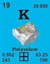
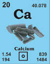
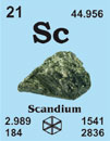
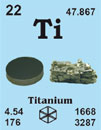
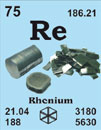
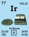
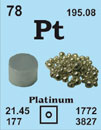
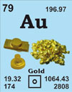
Übersicht der Elemente mit Zugang zu unserem Shop


Fax: +49 (0) 2461 - 9352 - 11